Detailed Guide On PCB Stencil For A Better Purchase Later
6th Apr 2021
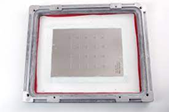
In layman’s term, pcb stencil is a sheet made out of stainless steel with some laser-cut openings. The main purpose is to place solder paste on PCB board for the proper surface mount component placement. The main goal of this stencil is to deposit the solder paste on given spots on any bare PCB board. It helps later to place the components in their exact places and aligned on board perfectly.
The main assembly process:
When it is time for assembling the PCB board, the solder paste needs to be added on the screen of the board. This paste is available in various framed stencils and even in prototype ones.
The picking and the right placement of the component can be done by hand or by machine.
Primarily, the reliable technicians will use tweezers for arranging the components and then placing them on board.
The tension, which is created by the solder paste, is enough to help keep the components in their right places.
You can use the pick and place machines sometimes for placing components on board.
Such machines will be using orientation information as held in given Centroid file to place the components on board with ease.
Ways the stencil is used:
Sometimes, the pcb stencil is aluminum and you can procure one which is already made from the hardware store or can try making one by yourself from the scratch. In the same way, you will order for readymade stencil from any manufacturing company. Before you start using one stencil for the upcoming PCB board, it is important to learn the importance it holds.
Perfect foil thickness:
The metals stencils on board will define the optimum foil thickness. Some examples might help you understand it better. Component packages like SOICs with 0.020” pitch will need one thin stencil for solder paste. Then, on the other hand, for components like 1206 or SOICs of around 0.050” pitch, the thick stencil is the one you should use.
Even though the thickness of the stencil generally depends on the solder paste deposition and it ranges from 0.001” to around 0.030 inches, the typical foil thickness that most of the PCB boards use will range from around 0.004” to 0.007”.
Now for the frameless stencils:
In case you are dealing with short runs or any prototype based PCB assembly, then the frameless stencils will present you with premium solder paste volume control.
This kind of stencil is purposely designed to work with the current stencil tensioning system.
These are mainly reusable stencil frames, which are also noted as universal frames.
As you are not going to glue the stencils permanently on the board, they are considered to be way cheaper than the framed ones.
Furthermore, these flexible stencil frames are also easier to store and won’t take up much space.
So, before you start using a stencil for PCB, it is important to log online and learn everything about the items in details.

