The formation of reliable solder joints in replacing a LGA package is critical to the proper replacement of such a device. The multitudes of pads present a challenge in producing an even solder line thickness. To this end, careful consideration must be applied to the stencil design. The stencil thickness, as well as the etched pattern geometry, determines the precise volume of solder paste deposited onto the device land pattern. Stencil alignment accuracy and consistent solder volume transfer is critical for uniform reflow-solder processing.
LGA stencil types come in a variety of configurations all of which can be used to rework an LGA location. These types include but are not limited to:
- A miniature LGA metal stencil which will print solder paste onto the PCB
- A miniature LGA plastic stencil with “repositionable” adhesive that allows for printing in tight spaces
- A polyimide LGA stencil placed on the bottom of a device which allows for the bumping of a part prior to placement
Miniature stainless steel LGA stencils are durable stencils which will mimic the initial manufacturing process and deposit a uniform volume of solder paste without smearing.
The optimum and reliable solder joints on the perimeter pads should have about 50 to 70 μm (2 to 3 mils) standoff height. Assembly studies on various LGA packages have shown that standoff height is primarily determined by thermal pad paste coverage. Area ratios and aspect ratios of 0.66 and 1.5, respectively, should not be exceeded, to maintain proper stencil design. The land pattern on the PCB should be 1:1 to the land pads on an LGA package. Maintaining a web thickness on the stencil between openings of 0.200 mm will allow space for flux volatiles to escape, thus minimizing voids.
An offshoot of this paste print and remove stencil is the peal and release adhesive backed plastic stencil. This LGA stenciling technique overcomes the problems associated with the mini metal stencils including their lack of coplanirty, the lack of getting even pressure and the resulting lack of consistency in pack volume in to each of the apertures. This stencil design insure that the stencil is intimate contact with the PCB with the added advantage of being able to be fitted in small spaces in a PCB.

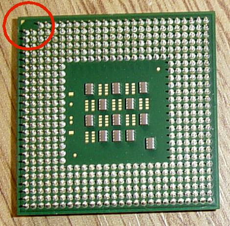
Example LGA Package
A new type of rework makes the job of reworking LGAs simpler by “bumping” the bottom of the device using a “bumping” stencil. After the leads on the bottom of the LGA are bumped the device is placed either using a rework system (just like you would place a reworked BGA) or a stencil placed on the board which “fits” the bumps onto the correct pad locations on the PCB. This results in less voiding on the center ground area of the part and lifts the part off higher from the PCB allowing for cleaning to more easily take place underneath the LGA.
